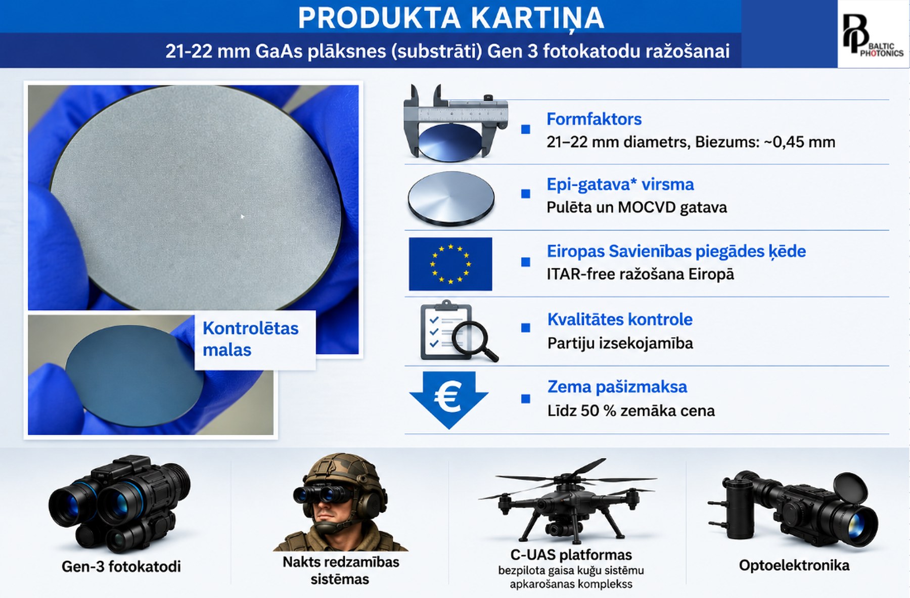
Baltic Photonics develops Latvian-made GaAs substrates for night vision technologies
SIA “Baltic Photonics”, in cooperation with SIA “Photonics International R&D center”, is implementing a commercialisation project co-financed by the European Union
SIA “Baltic Photonics”, together with its cooperation partner SIA “Photonics International R&D center”, is developing a project whose aim is to develop and validate a technology for the epitaxy and processing of specialised 21–22 mm gallium arsenide (GaAs) semiconductor wafers (substrates) for photocathodes, to produce a prototype series and a commercialisation plan, and to secure the supply of Latvian-made components to image intensifier manufacturers in Europe. Within the project, Baltic Photonics provides manufacturing capacity, market access and prototype testing, while Photonics International R&D center leads the creation and qualification of the supply chain, develops the initial epitaxy recipe and the outsourced MOCVD process, and prepares the commercialisation model.
Why it matters
GaAs photocathodes are the central element of modern night vision equipment – they provide high light sensitivity and make it possible to obtain a detailed image in darkness. At present the small-format substrates required for such photocathodes are obtained by cutting them from large 4–6 inch wafers, which causes edge defects, particle contamination and significant material losses. Moreover, the production of specialised 22 mm GaAs wafers is available neither in Latvia nor in the Baltics – European manufacturers depend on imports and are exposed to export control restrictions and geopolitical risks.
The approach developed in the project is fundamentally different: the substrates are grown directly in the target 21–22 mm format, with controlled edge processing and adapted MOCVD epitaxy. This makes it possible to substantially reduce the defect level and production costs – by up to 50% compared with current market practice – and at the same time to establish the first supply chain for this critical component localised in Europe, strengthening the competitiveness of the region’s photonics and electronics industries and Europe’s technological independence.
What the project will deliver
- establishing a European supply chain for substrate manufacturing (material procurement, cutting, polishing, marking);
- developing and optimising the MOCVD epitaxy process for small-format substrates;
- manufacturing and testing prototype series, validating them at a potential customer under real production conditions;
- preparing a commercialisation strategy and a techno-economic feasibility study;
- presenting the technology at international photonics and security technology exhibitions.
During the project the technology readiness level is to be raised from TRL 3–4 to TRL 6–7, reaching a validated solution that can be integrated into production. Specific interest in the new technology has already been confirmed by the only manufacturer of GaAs photocathodes in Europe, with whom a letter of intent has been signed.
Project information
- Project title
- Development of epitaxy and processing technology for specialised 22 mm GaAs semiconductor wafers (substrates) for photocathodes
- Application No.
- KOM/2025/17/P/1
- Programme
- LIAA commercialisation support – EU cohesion policy programme 2021–2027, measure 1.2.1.4 “Support for improving the technology transfer system” (project No. 1.2.1.4/1/23/I/001)
- Implemented by
- SIA “Baltic Photonics” in cooperation with SIA “Photonics International R&D center”
- Duration
- 12 months (from January 2026 to January 2027)
- Total costs
- EUR 551,940.58, of which the support funding is EUR 275,970.29 (50%)
The project is implemented within the field “Photonics and smart materials, technologies and engineering systems” of the Latvian Smart Specialisation Strategy.